Introduction
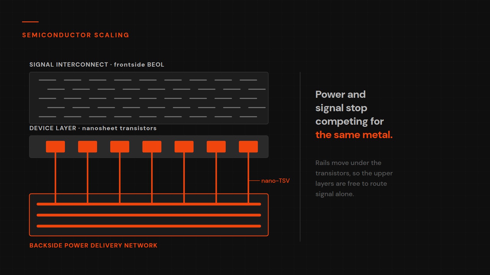
One of the most consequential breakthroughs in semiconductor manufacturing in 2026 is not a new material or a new transistor architecture — it is a fundamental rethinking of where power is delivered inside a chip. Backside Power Delivery Networks (BSPDN) are moving power routing from the front of the wafer — where it competes with signal wires for limited routing space — to the back of the silicon, completely separated from the signal interconnect stack.
In June 2026, imec and Sony announced a joint development of a backside interconnect integration module that brings this technology significantly closer to high-volume manufacturing. This development, combined with Intel's confirmed deployment of PowerVia (its BSPDN implementation) in Intel 18A, and TSMC's reported roadmap for backside power on N2P nodes, signals that BSPDN is transitioning from research curiosity to production-critical technology.
A word on vantage point. My work is on the other end of this supply chain: robotics, UAV and industrial-automation systems, and the software that runs them. I do not work in semiconductor process development, and this is not a first-hand account of integrating a backside power network — it is an engineer’s reading of what imec, Intel and TSMC have published, written by someone whose interest is in what eventually arrives on a board.
That interest is specific. Power delivery and heat are not abstractions when you are the one putting a compute module inside a sealed enclosure on a machine. They are the constraints that decide whether a design works in a factory in July. So the question I am actually asking of BSPDN is not “how clever is this” — it plainly is — but “what, if anything, does it change about the power and thermal problem I have to solve at the board and enclosure level?”
The Problem BSPDN Solves — Why Frontside Power Is a Scaling Wall
To understand why backside power delivery is significant, you need to understand the constraint it addresses. On a modern chip, the metal layers perform two functions: they carry signals between transistors and logic blocks, and they distribute power (VDD and GND) from the chip's power bumps to every transistor across the die.
As transistor density has increased with each node generation, the metal layers have become increasingly congested. Power rails — the wide metal lines that carry supply current — consume a significant fraction of the available routing tracks on the lower metal layers. This creates a direct conflict: the power rails needed to supply transistors consume the routing resources needed to connect those same transistors.
The consequences are measurable and significant: routing congestion forces logic cells to be placed further apart, reducing effective density. Power rail IR drop — the voltage loss along a resistive supply rail — increases as rails are made narrower to save routing resources. Higher IR drop means transistors at the end of the power distribution path see lower supply voltage, causing timing violations and performance loss. Fixing IR drop requires wider rails, which increases congestion further. This is a circular constraint with no good solution within the frontside routing stack.
Backside power delivery breaks this loop entirely by removing power rails from the signal routing layers.
How Backside Power Delivery Works
In a BSPDN implementation, the wafer is processed front-side as normal — transistors are formed, gate stacks are built, and the lower signal metal layers (M0, M1, M2) are deposited. At this point, rather than routing power through those signal layers, the wafer is flipped.
The back of the silicon substrate is thinned — dramatically, to just a few micrometers in advanced implementations. Vias are then etched through the thinned silicon from the backside to connect to the transistor source/drain contacts at the front. These backside vias (called buried power rails or nano-TSVs depending on the implementation) provide a direct, low-resistance power path from backside metal layers to individual transistors, entirely bypassing the signal routing stack.
The backside metal layers then distribute power across the die — using wider, lower-resistance rails that do not compete with signal routing because they exist on a completely separate plane of the chip.
The result: signal routing layers gain back all the tracks previously occupied by power rails. Transistor cells can be placed at higher density. IR drop decreases because backside power rails can be made wider without congestion penalty. Supply voltage uniformity across the die improves, enabling better timing closure and higher operating frequency.
The imec-Sony Backside Interconnect Module — What It Means in 2026
The imec-Sony collaboration announced in June 2026 focuses on a specific technical challenge in BSPDN implementation: integrating the backside interconnect module in a way that is manufacturable at volume with acceptable yield and process complexity.
The collaboration combines imec's deep expertise in advanced semiconductor process development — particularly in 3D integration, wafer bonding, and backside processing — with Sony's manufacturing experience and device integration capabilities. The focus is on developing a standardized backside interconnect module that can be adopted across different chip designs and process nodes, rather than requiring a fully custom BSPDN implementation for every chip.
This modular approach is significant because it addresses one of the key barriers to BSPDN adoption: the complexity and cost of adding backside processing steps to an already complex front-end process flow. A standardized module reduces the per-design engineering effort and provides a validated, manufacturable baseline.
For the electronics engineering community, this development signals that BSPDN is no longer confined to large, vertically integrated IDMs like Intel. The path to BSPDN for fabless chip designers using foundry services is becoming clearer.
Intel PowerVia — The First Production BSPDN Implementation
Intel's PowerVia is the most mature BSPDN implementation in the industry as of mid-2026. Validated on Intel 18A test vehicles, PowerVia demonstrated meaningful improvements in routing congestion reduction and supply voltage uniformity in published data.
Intel's implementation uses nano-scale through-silicon vias (nano-TSVs) to connect backside power rails to transistor contacts, with the silicon thinned to sub-10 micrometer thickness to minimize via resistance. The backside rail stack uses a dedicated metal layer optimized for power distribution rather than signal routing.
Intel 18A, targeting production in 2026, is the first node where PowerVia is integrated with Intel's RibbonFET gate-all-around transistor architecture. This combination — GAA transistors plus backside power — represents the two most significant process innovations Intel has combined in a single node, and puts Intel's process technology back in competitive contention with TSMC N2 on transistor density and performance metrics.
System-Level Implications for Electronics and Mechatronic Design
For engineers working at the system level — designing boards, selecting SoCs, specifying FPGAs — BSPDN matters in several ways that will become increasingly relevant over the next 2–4 years.
First, chips manufactured on BSPDN nodes will achieve better performance at lower power. Lower IR drop means more uniform transistor performance across the die, enabling higher clock frequencies without increasing supply voltage. For high-performance edge AI chips used in industrial automation — the processors running inference on factory floor edge devices — this translates directly to more inference operations per watt, enabling more capable models in thermally constrained enclosures.
Second, higher transistor density on BSPDN nodes means more compute in smaller die area, which translates to smaller SoC packages and reduced PCB area for equivalent compute performance. For compact embedded controllers and mechatronic devices where board space is at a premium, this matters.
Third, improved supply voltage uniformity across the die will reduce clock frequency variability, which has implications for timing-critical embedded systems. Chips from BSPDN nodes should show tighter performance bin distributions and more predictable behavior at the high end of their frequency range.
The Lithography Requirements for BSPDN — Connection to EUV and High-NA EUV
BSPDN implementation at advanced nodes requires lithography capable of printing the nanoscale vias that connect backside metal to transistor contacts. At 2nm and below, the backside via pitch is in the range of 20–30nm, which requires EUV lithography for the via patterning steps.
High-NA EUV (Numerical Aperture 0.55, implemented in ASML's EXE:5000 and EXE:5200 systems) becomes relevant for the most aggressive BSPDN implementations at sub-2nm nodes, where the via pitch shrinks further. ASML's High-NA EUV tools, which began pilot line deployment at Intel and TSMC in 2025-2026, provide the resolution needed to pattern features at these dimensions with acceptable process margin.
The intersection of BSPDN and High-NA EUV represents the dual-axis of semiconductor scaling for the remainder of this decade — new interconnect architectures enabled by ever-more-capable lithography.
What it does and does not change at the board and enclosure level
Backside power delivery solves a problem inside the die. It is worth being precise about the fact that the problem I have to solve sits several layers above it, and does not go away.
What genuinely improves downstream is the quality of the power the transistors receive. Reduced IR drop and a cleaner supply mean a part behaves more consistently at its rated frequency, and the resulting efficiency gains can show up as a slightly better performance-per-watt figure in a datasheet. For anyone specifying a compute module against a power budget, that is a real, if incremental, benefit.
What does not change is everything outside the package. The board still has to deliver clean power to the part, with the decoupling, plane design and transient response that demands. The enclosure still has to move the resulting heat somewhere, often without fans, often sealed against dust and moisture, often in an ambient temperature no data centre would tolerate. A chip that is more efficient at the die level does not relieve the thermal design of a cabinet that sits next to a furnace — and in practice, efficiency gains at the silicon level have a habit of being spent on more capability rather than banked as lower power.
There is a second-order point worth flagging honestly, because it cuts the other way. Separating power and signal into different sides of the wafer is a significant manufacturing change, and manufacturing changes take time to show up as mature, well-characterised, long-lifecycle parts. Industrial designs care about that maturity more than they care about the newest structure. Early availability at the leading edge and availability in the parts an automation designer can actually specify are years apart.
My general position is that the physical layer of a machine should be designed against its own requirements and its own failure modes — power loss, thermal excursion, brownout, an actuator drawing more than expected — and that improvements in silicon should be treated as headroom, not as a substitute for that design work. BSPDN is a good example: welcome, real, and entirely upstream of the constraints that actually decide whether a machine survives its environment.
Conclusion
Backside Power Delivery Networks are not incremental — they are a structural change in how a chip is built, breaking a scaling constraint that front-side routing had made unavoidable. The imec–Sony backside interconnect module announced in June 2026, Intel’s PowerVia deployment in 18A, and TSMC’s roadmap for backside power beyond N2 together mark the point where this stops being a research topic and becomes production architecture.
From the machine side, the right expectation is modest and specific: over the next several years, compute parts with somewhat better and more consistent performance per watt. That is useful. It is not a change to the power integrity work on your board, or to the thermal design of the box that board lives in — which is where, in my experience, the difficult engineering in a deployed system actually is.