Introduction
Gallium Nitride (GaN) power semiconductors are undergoing rapid adoption in industrial power electronics in 2026, driven by a combination of maturing device technology, improving cost competitiveness, and application performance requirements that silicon MOSFETs simply cannot meet. From motor drives in industrial automation to switching power supplies for AI data centers to power converters in electric vehicle charging systems, GaN is transitioning from an emerging technology to a production-ready alternative that demands serious engineering consideration.
At Embedded World 2026 and across the electronics industry press in June 2026, GaN has been prominently featured — particularly in the context of ScaleBridge Labs, an incubator launched in October 2025 specifically focused on GaN technology development and commercialization. The investment in GaN-specific incubation infrastructure is a clear market signal: the industry is treating GaN power electronics as a strategic technology category, not a niche specialty.
I should be precise about the basis for this one. I have studied industrial motor-drive architecture and power electronics from a mechatronics and automation perspective — the perspective of someone who specifies and integrates drives as part of a machine. I have not designed or deployed a GaN-based motor drive, and nothing in this article should be read as a report of measured results or field experience with these devices.
What follows is therefore an engineering analysis rather than a deployment account: the device physics, the performance characteristics that follow from it, the design challenges that come with them, and a framework for thinking about where the trade lands. Where the practical implications are genuinely uncertain from the outside, I say so.
Why Silicon MOSFETs Are Hitting Physical Limits in High-Performance Power Applications
Silicon power MOSFETs have been the dominant switching device in power electronics for four decades. They are well-characterized, supported by mature gate driver ecosystems, available in an enormous range of voltage and current ratings, and cost-effective at high volumes. None of this is changing. But silicon has fundamental material limits that create performance ceilings that GaN does not have.
The relevant material properties for power electronics are: bandgap energy (higher is better for blocking high voltage), electron mobility (higher enables lower on-resistance for the same device area), critical electric field (determines breakdown voltage for a given device thickness), and thermal conductivity (determines heat removal capability). Silicon's bandgap of 1.1 eV and critical field of 0.3 MV/cm set hard limits on the blocking voltage and specific on-resistance achievable for a given device size.
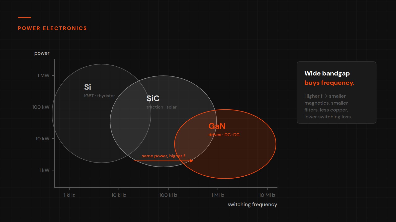
At switching frequencies above 100 kHz, silicon power MOSFETs suffer from significant switching losses driven by their output capacitance and reverse recovery charge. These switching losses generate heat that must be managed thermally, require heat sink mass that increases system size and weight, and impose a fundamental power density limit on silicon-based power converters. This is the ceiling that wide-bandgap semiconductors — GaN and SiC — are designed to overcome.
GaN Power Device Physics — What Makes It Different
Gallium Nitride has a bandgap of 3.4 eV (versus 1.1 eV for silicon) and a critical electric field of 3.3 MV/cm (versus 0.3 MV/cm for silicon). These properties translate directly to performance advantages: GaN devices can block the same voltage as silicon devices in one-tenth the thickness of semiconductor material, which dramatically reduces the on-resistance and therefore the conduction loss.
The dominant GaN power device structure used in industrial applications is the GaN HEMT (High Electron Mobility Transistor) — specifically the lateral GaN HEMT grown on silicon or SiC substrates. The HEMT structure exploits the two-dimensional electron gas (2DEG) formed at the interface between GaN and aluminum gallium nitride (AlGaN) layers — a naturally occurring sheet of free electrons with extremely high mobility. This 2DEG forms the conductive channel of the transistor and can be depleted or enhanced by the gate voltage.
The practical performance consequence of GaN HEMT physics: at 650V blocking voltage, GaN HEMTs achieve specific on-resistance (on-resistance multiplied by active area) of 1–3 mΩ·cm², compared to silicon MOSFETs at 50–100 mΩ·cm² at the same voltage rating. This 10x to 50x advantage in specific on-resistance translates directly to smaller die area for the same on-resistance target, lower conduction losses, and lower switching losses (because output capacitance scales with die area).
The absence of a body diode with stored charge (no p-n junction in the lateral GaN HEMT structure) eliminates reverse recovery losses entirely — a significant advantage in bridge circuit topologies (H-bridge motor drives, totem-pole PFC, LLC resonant converters) where silicon MOSFET body diode reverse recovery generates substantial switching losses and causes voltage spikes that require increased drain voltage headroom.
Performance Advantages in Industrial Motor Drive Applications
Industrial motor drives — the power electronics that control AC induction motors, permanent magnet synchronous motors (PMSM), and brushless DC motors in factory automation, robotics, conveyors, pumps, and compressors — are a primary target market for GaN power devices in 2026.
The switching frequency of a motor drive directly determines the quality of the output current waveform (higher frequency = smoother current = less motor heating and torque ripple) and the size of the output filter inductor (higher frequency = smaller inductor). Silicon MOSFET-based drives typically switch at 4–20 kHz for industrial motors — a compromise between switching loss (which increases with frequency) and filter size.
GaN-based motor drives can switch at 100 kHz to 500 kHz with switching losses significantly lower than silicon at 20 kHz. This enables: dramatically smaller output filter inductors (1/10 to 1/25 of the size at the same inductance value and ripple current), better motor current waveform quality (lower harmonic content, lower torque ripple, lower motor heating), faster dynamic response (the current control loop can operate at much higher bandwidth when the switching frequency is higher), and overall system size reduction.
In robotics motor drives — where every gram and millimeter of volume matters for actuator design — the ability to shrink the power stage by 5x to 10x by moving to GaN switching frequencies is transformative for system integration. A servo drive that previously required a separate power electronics module can be integrated directly into the motor housing when the power stage is implemented with GaN.
Design Challenges — What Engineers Must Address with GaN
GaN power devices are not drop-in replacements for silicon MOSFETs. Their superior switching performance creates new design challenges that must be addressed for reliable, high-performance operation.
Gate Drive Requirements: GaN HEMTs have very low gate capacitance and switch extremely rapidly — rise and fall times of 1–5 ns are typical for enhancement-mode GaN devices at 650V/100A ratings. This rapid switching generates high dV/dt (voltage rate-of-change) at the switching node — hundreds of V/ns in some applications. Gate drive circuits must be carefully designed with low-inductance layouts and appropriate gate resistance selection to control switching speed and prevent oscillation without excessive switching loss.
PCB Layout: The high switching speeds of GaN require much more careful PCB layout than silicon MOSFET designs. Parasitic inductance in the commutation loop — the layout loop through the high-side switch, low-side switch, and DC bus capacitors — causes voltage overshoots at the switching transitions. For GaN operating at 650V bus voltage, even a few nanohenry of loop inductance can cause overvoltage spikes that exceed the device's voltage rating. Multi-layer PCB designs with minimized power loop area, X2Y capacitors placed as close as possible to the device, and power stage co-packaging are all required for robust GaN converter design.
Enhancement-Mode vs. Depletion-Mode: Native GaN HEMTs are normally-on (depletion-mode) — they require a negative gate voltage to turn off. This creates a reliability concern in power electronics (if gate drive power fails, all switches turn on simultaneously — a catastrophic condition). The industry has largely addressed this by offering enhancement-mode (normally-off) GaN HEMTs through various techniques: cascode configuration (a low-voltage silicon MOSFET in series with the GaN device), p-GaN gate (using a p-type GaN layer to raise the threshold voltage positive), or recessed gate structures. Enhancement-mode devices are the standard choice for industrial power designs.
When to Choose GaN Over Silicon — A Design Framework
GaN power devices provide clear advantages in specific application conditions. The decision framework for choosing GaN over silicon should consider these criteria:
Choose GaN when: switching frequency above 50 kHz is required or beneficial; power density (kW/liter or kW/kg) is a primary design constraint; thermal management is a critical challenge and reducing switching losses would meaningfully improve it; output filter size reduction would provide significant system-level benefit; reverse recovery losses from silicon body diodes are causing performance or EMI problems in a bridge topology; and the application is in the 200V–650V range where GaN is most mature (1700V+ applications are more appropriate for SiC).
Stay with silicon MOSFET when: switching frequency is below 50 kHz and silicon switching losses are acceptable; cost is the dominant constraint and GaN premium is not justified; the application voltage is below 100V where silicon performance is highly competitive; the engineering team does not have GaN layout expertise and the development timeline does not allow learning; or the system uses existing silicon-optimized designs that would require significant redesign effort.
The ScaleBridge Labs GaN Incubator — What It Signals for the Industry
The launch of ScaleBridge Labs in October 2025 as a GaN-focused technology incubator and accelerator is a market indicator worth noting. The emergence of a dedicated GaN incubation infrastructure — providing access to GaN process technology, device characterization facilities, and industry network connections — signals that the investor and industry community views GaN power electronics as having the characteristics of a platform technology: multiple application domains, significant market opportunity, and a need for specialized infrastructure to accelerate development.
This is the ecosystem maturation phase of a power semiconductor technology — the phase after the foundational technology is proven but before commodity cost and widespread engineering familiarity are established. Engineers who develop GaN design expertise now are positioning themselves on the right side of this adoption curve.
What draws my interest — stated as analysis, not experience
Since I have not built with these devices, the useful thing I can offer is why a mechatronics engineer looks at them at all, and what I would want to establish before committing a design to one.
The interest is in the switching behaviour and what follows from it. Higher switching frequency, lower switching losses and the absence of reverse recovery are not interesting as specifications; they are interesting because of what they permit further up the system. Higher switching frequency shrinks the magnetics and filtering, which is a size and weight argument. Lower losses mean less heat to remove, which in a sealed industrial enclosure is often the binding constraint rather than the electrical performance. For a robotic actuator, where the drive electronics may have to live on or near a moving structure, power density stops being a preference and becomes an architectural enabler.
What I would want to resolve before designing one in is essentially the other half of the article. The layout sensitivity and gate-drive requirements mean the device is less forgiving than the silicon part it replaces, and that has organisational consequences as well as technical ones: it changes who needs to be involved, how much board-level iteration to budget for, and how much EMI work sits between a working prototype and a compliant product. Those costs are real and land early, while the benefits land in the finished system.
My general approach applies here as much as anywhere: start from the requirements and the failure modes, then choose the technology. If a design genuinely needs the power density or the thermal headroom, the case is strong and the additional engineering is the price of it. If it does not, a well-understood silicon design that the team can execute confidently is very often the better engineering decision, whatever the newer device can do on paper. That is the same reasoning I would apply to a communication protocol or a compute platform, and I do not think power electronics is an exception.
Conclusion
GaN power semiconductors are not the future of industrial power electronics — they are the present. With 650V enhancement-mode GaN HEMTs commercially available from Infineon, Texas Instruments, GaN Systems (now Infineon), EPC, and Navitas, the devices are production-ready and supported by mature gate drive solutions and design resources. The performance advantages — higher switching frequency, lower switching losses, zero reverse recovery, smaller passive components — are real and demonstrated in production systems.
The learning curve is real: GaN demands more careful PCB layout, gate drive design and EMI management than silicon, and those are not incidental details — they are the difference between the device delivering its advantages and misbehaving. For industrial motor drives, robotics actuators and high-density power supplies, where power density, efficiency and size are genuine differentiators, that engineering investment is what the technology asks of you in exchange for what it offers. Whether the exchange is worth making is a judgement each design has to reach on its own requirements.